|

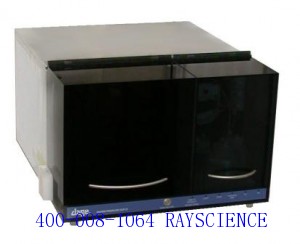
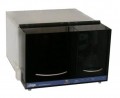
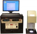
CVP21 with footprint 60(W)*80(D)*195(H)cm,
to minimize space requirements in clean room.
|
CVP21 is the COMPLETE SOLUTION: CVP21 supports the COMPLETE spectrum of materials:
-
Group IV semiconductors as Silicon (Si), Germanium (Ge), Silicon Carbide (SiC), or
-
III-V semiconductors as Gallium Arsenide (GaAs), Indium Phosphide (InP), Gallium Phosphide (GaP), ..., or
-
ternary III-V alloys as Aluminum Gallium Arsenide (AlGaAs), Gallium Indium Phosphide (GaInP), Aluminium Indium Arsenide (AlInAs) ..., or
-
quaternary III-V alloys as Aluminum Gallium Indium Phosphide (AlGaInP), ..., or
-
Nitrides, as Gallium Nitride (GaN), Aluminum Gallium Nitride (AlGaN), Indium Gallium Nitride (InGaN) or Aluminum Indium Nitride (AlInN), or
-
II-VI semiconductors as Zinc Oxide (ZnO), Cadmium Telluride (CdTe), Mercury Cadmium Telluride (HgCdTe, MCT)..., or
-
less commonly used semiconductors (please contact us for sample measurements).
CVP21 supports the COMPLETE sample range:
-
Stacked layers are no problem (the material, the doping and the doping type may vary).
-
No Restrictions concerning the substrate (may be conductive or insulating).
-
Sample size: 4*2 mm?to complete 8" wafer size are standard (smaller samples on request).
CVP21 supports the COMPLETE resolution range:
(*) may depend on material type/ sample quality. Please ask for sample measurements
CVP21 comes as a COMPLETE measurement system:
-
High Reliability system (special concern on electronics, mechanics, optics and fluid system).
-
Calibration-free system (Complete self calibrating electronic system - no needs for cable capacitance calibration).
-
Easy-to-use (Software optimized with full user management - easily used as well in production as in laboratory environment).
-
Wafer-Stepping (Complete wafer stepper is optionally available - to process several measurements on a wafer in full automation).
-
Camera-Control (The process is controlled on-line by a color camera - after each measurement camera data is available in film strip format).
-
Recipes (Measurement recipes are pre-defined and may easily modified by a user with higher priority).
-
Dry-In / Dry-Out: Auto-Load / Unload / Reload (The loading/ un-loading and re-loading of the electrochemical cell is automated and may be easily modified by a user with higher priority. The samples are processed dry-in / dry-out).
|